Characteristics
First, the basic properties and functions of the boost converter are to be investigated, for this a voltage source of $U_{source}=20V$ is connected to the input of the module optimizer, the output is wired with an ohmic resistor of $R_{L} = 24 \Omega$. The duty cycle is set to $d=35\%$, this would correspond to an output voltage of $U_{out}=30.77V$ according to equations on basics chapter boost converter. The practical measurement shows an output voltage of $U_{out}=29.7V$ which seems reasonable with consideration of conduction and switching losses and the voltage drop of about $0.4V$ of the Schottky diode MBRB1060. Of further interest is the ripple of the output voltage which is examined with an oscilloscope. A plot of the output rippe voltage is shown in figure. The output voltage delta of $\Delta U_{out}= 0.1V$ selected in the design is $\Delta U_{out_{mess}}=0.146V$ in the measurement and is thus $46mV$ greater than required. However, this does not affect the function of the module optimizer.
Output ripple voltage
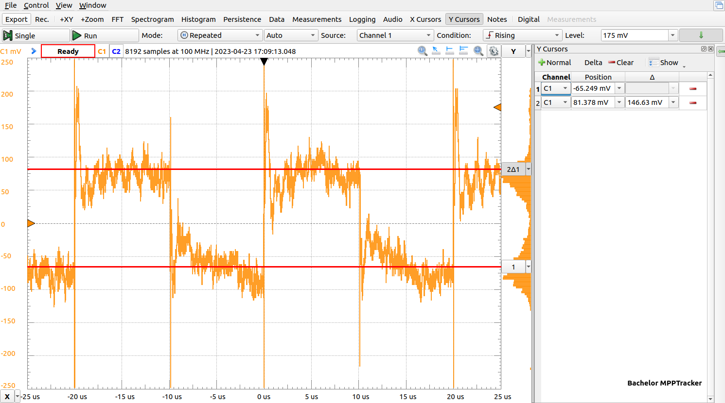
The measurements show a DC rms value of $V_{dc_{eff}}=29.7V$ and an AC rms value of $V_{ac_{eff}}=47.6mV$, giving a ripple of $0.16\%$ according to \eqref{eq:schwingungsgehalt}.
\[\label{eq:schwingungsgehalt} r_{u} = \frac{V_{ac_{eff}}}{|V_{dc_{eff}}|} = \frac{0.0476V}{29.7V} = {1.6e-3}\]Next, the characteristic curve of the PV-emulator is to be recorded, for this the VI-scanner algorithm is used and extended by the recording function of the measured data to a SD-card, furthermore the duty cycle is set directly, thus the PI-controller is not used. The PV emulator is operated with a current source with a limitation of $I=5A$, the VI characteristic can be seen in pv emulator characteristics figure and shows the typical characteristic of an PV-module. In addition, the power is shown on another axis, from which the global MPP can be easily read. This experimental test of the characteristic curve recording shows the general functionality of the basic functions of the solar module optimizer, in particular the measurement of voltage and current at the solar module, the control of the duty cycle for the boost converter and the processing of the collected data.
PV emulator characteristics

The VI curve with one third of the solar module shaded is shown in shaded figure. Here, the PV emulator is used again, but with the configuration of two current sources $I_{1}=5A$ and $I_{2}=2A$ and the two bypass diodes, where current source $I_{1}$ is connected to diodes $D_{1}$ to $D_{20}$ and current source $I_{2}$ is connected to diodes $D_{21}$ to $D_{30}$. The VI-characteristic shows here a clearly changed course of the current over the voltage, already at a voltage of approx. $V_{pv}=14V$ the current breaks down from $I_{pv}=4A$ to $I_{pv}=2A$.
While only one global MPP appears in the PV-characteristic in the experiment without shading from figure, two MPP become visible here. These two MPP are also called local MPP and are the challenge for the next chapter compasion, where the two algorithms are tested and compared.
PV emulator characteristics shaded
