Snubbercircuit
If an inductor is switched with a mosfet, it can lead to significant voltage overshoots during the switch-off time and the switch-on time. When the mosfet switches off, the current of the load $iL$ drops towards zero. This causes the voltage $U_{DS}$ across the mosfet to increase to a large value due to the phenomenon $Ldi/dt$, where $L$ can be the line inductances of the drain and source lines. Under certain conditions, the mosfet can be destroyed in this way. To slow down the change of voltage at the mosfet, a capacitor $C$ is connected across the mosfet according to figure. The capacitor fixes the problem of voltage spikes, but causes a new problem during the switch-on time. When the mosfet switches on again, the capacitor is discharged via the mosfet and this causes a large discharge current spike that can also destroy the unit.
Capacitor snubber

To limit the current, the resistor $R$ is connected in series with the capacitor. However, the resistor is only to limit the current during the on time, it is not required during the off time. To reduce the losses during the switch-off time, a diode $D$ is connected in parallel to the resistor. Thus, the resistor $R$ only shows its effect during the switch-on phase, as shown in snubber circuit.
Snubber circuit

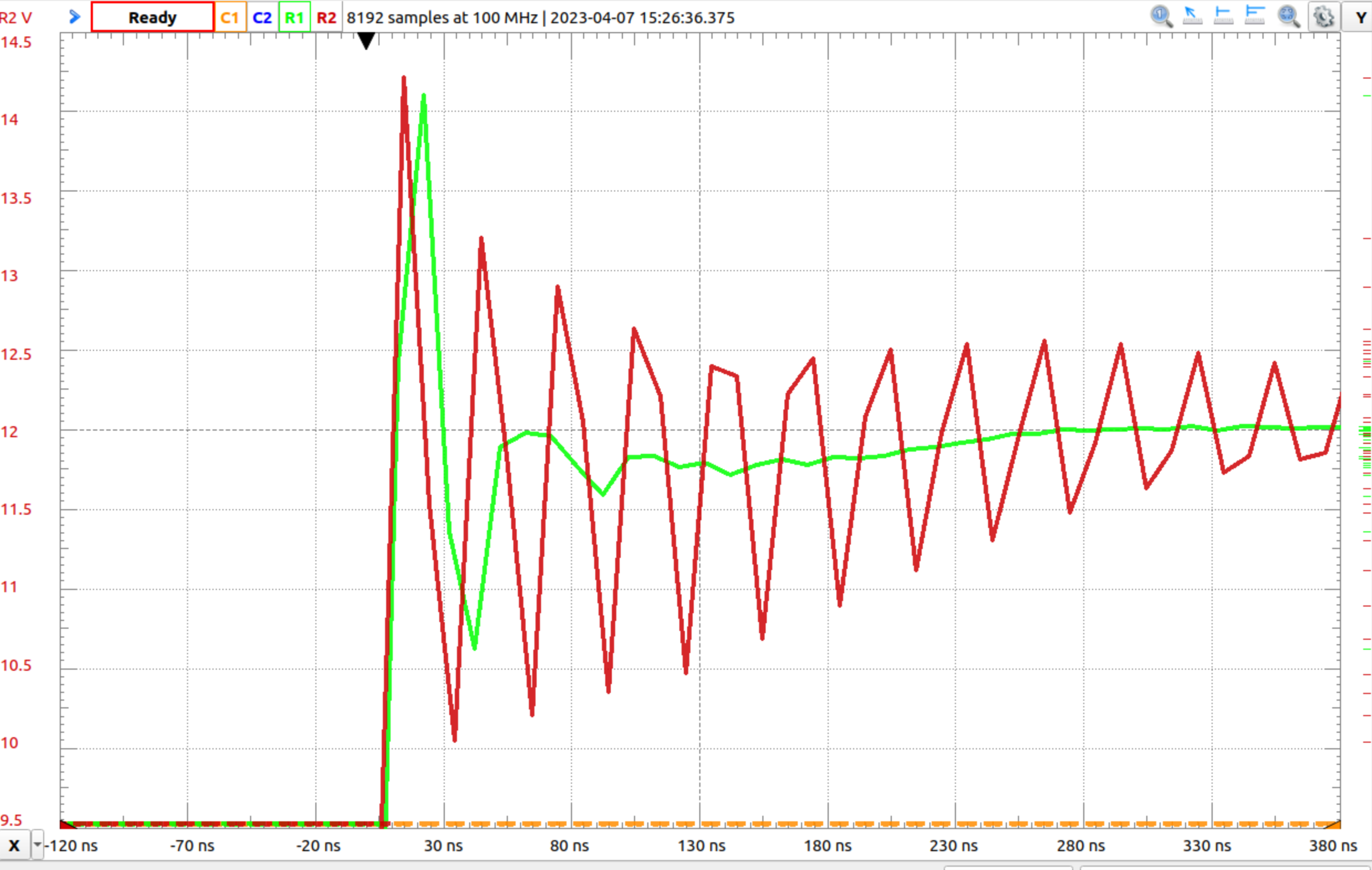
There are different ways to determine the values for $R_{snub}$ and $C_{snub}$. Here, a way will be shown that is based on the assumption that the parasitic inductances of the supply lines and the capacitances of the free-wheeling diode of the mosfet form an RLC filter that resonates at a certain frequency. The basis for the procedure is the measurement of the resonance frequency with an oscilloscope. The course of the measurement is shown in red in figure. The resonant frequency of $f_{c} = 31.25 Mhz$ is determined from the period of the oscillation. Then the dominant part of the circuit is determined. The inductance of the supply line is dominant if it is a low-side switch. The capacitance of the body diode of the mosfet or the capacitance of the free-wheeling diode is dominant if it is a high-side switch. The solar module optimiser works as a low-side switch, so the quantity sought is the parasitic inductance of the supply line and the capacitance of the free-wheeling diode can be neglected. The parasitic inductance is determined with the help of an impedance analyser, which is connected to the input terminals of the circuit and measures the impedance at different frequencies. The measurement shows that at the resonance frequency the parasitic inductance is $L_{para} = 10nH$. With the equation \eqref{Rsnub} the value for the resistance $R_{snub}$ is determined.
\[\label{Rsnub} R_{snub} = 2 \pi f_{c} L_{para}=2\cdot\pi\cdot31,25 Mhz\cdot10 nH = 1,96 \Omega\]The capacitor \(C_{snub}\) can be chosen large for high damping, but this also increases the losses in the capacitor during the switching process. Therefore, the maximum power loss is set to $P_{loss} = 60mW$ when using 0805 package SMD components. The equation \eqref{Csnub} calculates the maximum capacitance for the snubber capacitor considering the power dissipation. The voltage applied to the capacitor is measured as $U_{C_{snub}}=25V$ and the switching frequency is $f_{s}=50 kHz$.
\[\label{Csnub} C_{snub} = \frac{P_{loss}}{U_{Csnub}}^{2} \cdot {f_{s}} = \frac{60 mW}{(25V)}^{2} \cdot {50 kHz} = 1,92 nF\]The figure shows the voltage $U_{DS}$ across the mosfet measured with an oscilloscope, without snubbercircuit in red and in comparison to this with the snubbercircuit of the calculated values in green. A considerable damping of the oscillation can be observed [@biricha].
Snubber ringing
 Note: poor picture Nyquist–Shannon sampling theorem violated